Since a bus is basically just a highway between two devices, there is always a directionality implicit in the transfer, that is, there is always a sender and one or more receivers. One component has to initiate the transfer and it usually does this by asserting logic values on the control wires. The receivers pay attention and notice changes in the values. We call the sender the initiator because it initiates or starts the activity. The other device is called the responder because it waits until the activity starts and it receives a start signal.
If more than one component tries to control the bus by setting the control wires to different logic values, then chaos will result. Thus, only one device can be in control at any point of time, that device is called the bus initiator. The device to which the control signals are directed is called the bus responder. These roles flip back and forth, as one device might be the initiator for one transfer and the responder for the next. It is also possible for there to be multiple responders in a single bus operation.
Terminology that was once thought colorful and evocative has since changed due to the desire to include everyone and not conjure up images of a dark past. Such is the case with the issue of coordination between computer devices. While we used to call an initiator device the "master", the the responding device the "slave," such terms are now eschewed, no matter how cute or even accurate they once were thought to be. Be aware that in many hardware textbooks you may see the terms bus master and bus slave.
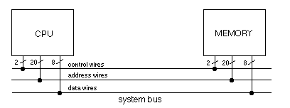
Fig. 16.4.1 shows the CPU and the main memory connected to a system bus. The slashes across the wires indicate how many wires there are: 2 control, 8 data and 20 address. This keeps the huge amount of detail in the diagram down to a minimum.
To perform a read operation, the CPU takes the lead by putting an address of the desired byte on the address wires, and setting both control wires MA and RD to 1. The memory is designed to watch for MA to go high, at which point it absorbs the operation code (RD) and the address and begins to decode that address. After a delay, it puts the desired byte onto the data wires, which the CPU absorbs. In a tightly coupled system, the exact timing between the CPU and the memory is well defined and those two circuits "know" how much time they have to wait. In a more heterogeneous system, other mechanisms must be used.
During a read operation, the CPU acts as the initiator while memory always acts as the responder, even though the data is flowing from memory to the CPU during the latter part of the operation. The identification of who is the initiator and who is the responder depends upon which component starts the bus operation by putting values on the control wires. Since memory never takes the lead in this way, it is always the responder.
A memory write operation starts with the CPU asserting MA=1 and RD=0, putting the address where to write the byte on the address wires, and the actual byte to write on the data wires. The memory responds internally when it "sees" MA is 1 and it absorbs all these values and stores the value. In some cases, the CPU may simply start the memory on a write and then go off to do other useful work. For a read, however, the CPU must wait the full amount of time for the memory to fetch the desired value.
Thus, we have seen that there are several logical operations on buses, even though the data is always just flowing between two devices in one direction. The read operation saw data flowing in both directions, while a write has data flowing in just one direction, from CPU to memory.