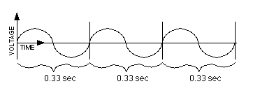
Fig. 16.6.1: Sine wave representing clock pulses
3 Hz = frequency, 1/3 seconds = the period
Buses have to solve a very thorny problem that does not arise within the CPU, which is how to coordinate electronic events. Within the CPU, the designer can simply make sure that the longest data path governs the maximum amount of time it takes for signals to travel from one end of the logic circuit to the other. In a bus, many diverse components must fit together and work without interference, and they cannot be manufactured to be in perfect accordance with each other's timing.
So a mechanism from the world of music is used -- the conductor. In a symphony orchestra, the conductor stands on a podium where all the musicians can see him or her. By waving a wand in rhythmical fashion, the conductor establishes a beat which is used to coordinate the timing of all the events in the orchestra. The violins, for example, see a sheet of music in front of them divided into bars filled with beats. These bars and beats divide time up into units so that music can progress. It is the job of the conductor to say, by waving the wand, just exactly how long a single beat lasts.
Electronic circuits are not musical by nature, although many fabulous things are done nowadays with digital synthesizers, but there needs to be a conductor that establishes a beat. A special device called a clock generates a series of pulses which are used like the beats of a conductor. Other circuits change their state by synchronizing with the pulses coming out of the clock. (To synchronize means "to come together in time," and means in general to coordinate two or more actions so that they happen at the same time.)
Clocks in computers are formed by applying electric current to certain crystals. Quartz is often used for this purpose. When electricity is applied to a quartz crystal, it expands and contracts rhythmically as the electrons travel through it. This rhythmical change in the shape of the crystal can be used to cause changes in the voltage, thereby emitting a series of on/off pulses at a very high frequency. When you buy a new Pentium that has a 166 MHz clock, you are buying a computer with a clock that pulses 166 million times per second.
Frequency refers to how often cyclical changes occur within a specified time unit. Frequency is measured in Hz, which is pronounced "hurts" and comes from Heinrich Rudolph Hertz, a German physicist (1857-1894) who studied electromagnetic radiation. Period refers to how long one complete cycle takes, and is the reciprocal of frequency. These terms apply to events or signals that recur repeatedly, or periodically.
For example, suppose that you get 12 paychecks in a year and they are equally spaced in time. Thus, the frequency of getting paid is 12 cycles per year, where cycle is hereby defined to be the time between pay periods. The period is how long one cycle lasts, and is 1/12 (one twelfth) of a year in this example.
Similarly, if a computer's clock pulses 166 million times per second, that is the frequency, 166 million cycles per second. One complete cycle is comprised of a time when the signal changes to a certain voltage level and then drops to another. Fig. 16.6.1 shows this as a smooth sine wave:
Fig. 16.6.1: Sine wave representing clock pulses
3 Hz = frequency, 1/3 seconds = the period
To say that the frequency is 166 million cycles per second, or 166 million Hz, means that the upper and the lower bumps form one cycle and repeat themselves 166 million times every second. Thus, the period of one cycle is 1 divided by 166 million, which is 0.0000000060241 seconds or 6.0241 nanoseconds.
Every system bus has its own clock which dictates how fast signals can change on the wires of the bus. Components which attach to the bus must obey the clock and perform their actions within the time cycles dictated by the bus's clock. There are other clocks within the attached components: the CPU has its own internal clock which regulates how fast it performs instructions, and the various I/O devices have their own clocks, and memory may have its own clock. But all components have to obey the clock of the system bus if they wish to use this common pathway.
In the following discussion we will look at a hypothetical bus and discuss how timing signals work on it as the CPU communicates with memory. Keep in mind that what we will be studying is a vastly simplified version of real buses.
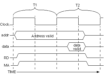
Fig. 16.6.2 shows a timing diagram for the bus when a read operation is occurring:
This is really a graph showing activity on the various wires of the bus over time. Some wires are single lines, such as RD, MA and Clock. There are two voltage levels: high and low, with high being used to represent logic 1 and low being used to represent logic 0. The clock cycles back and forth between logic 1 and logic 0.
Other wires such as data and address consist of a group of wires. Since drawing 16 or 32 or 20 wires, some going high and some going low, would unnecessarily clutter the diagram, we shall use a standard convention in these types of timing diagrams; whenever valid data (logic values which we are interested in) are present on these wires, we draw an elongated diamond shape. This can be seen above on both the address and data wires. Remember that there are 1s and 0s on these wires all the time that the power is on, but they are not valid or interesting 1s and 0s until the diamond starts.
All the signals except the clock above show another convention that seeks to imitate physics, namely that when a signal changes from low to high or high to low, there is a slight slope as it moves to its new value; it does not change instantaneously. In reality, no wire ever changes its voltage level instantaneously due to the inertia of the electrons. The clock signal is shown as a sharp "square wave" only because it changes from low to high and vice versa in a much shorter time span than the other signals.
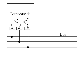
The bus's clock is what generates the clock signals above. The bus initiators and responders are set up to put new values on the wires and read values off the wires only at certain moments of time, always on a transition of the clock from high to low. This is done because the values on the wires must be copied into flip flops at the junction between the bus and the component. Then the component copies the values out of the flip flops into its other circuitry. Recall that flip flops are edge-triggered memory devices, which means they latch the new value into their memory only when the control wire makes a change in voltage level (and only in one direction.) Therefore, we assume that all the interface registers, which are arrays of these flip flops between the bus and the component, are negatively edge-triggered, i.e. they latch the new value only when the bus clock pulse goes from high to low.
Fig. 16.6.3 reinforces the idea of registers as go-betweens for the bus and the components.
The above bus is called a synchronous bus because all its actions are coordinated by the uniform bus clock signal. Activities such as getting values off the bus can only happen during the transition of the time signal, though some components may put new values onto the bus at other times. But no component "reads" values off the bus until the clock signal makes its downward transition, even though the correct values may be available sooner than that. Synchronous buses are easier to build and debug, although they are a little slower than their cousins, asynchronous buses.
Let's go through Fig. 16.6.2 very carefully. After time cycle T1 begins, the CPU begins a read transaction with the memory by setting the address wires to the desired value. Of course, the CPU has already been cleared to do this by the arbiter. In an earlier time phase, not shown in Fig. 16.6.2, the CPU asserted its bus request line and the arbiter decided that it could be the one to control the bus next by asserting the CPU's bus grant line.
The CPU next asserts RD and MA as a way of saying it wants to read and that the memory should become active. All components attached to the bus latch these bus values into their interface registers at the falling edge of T1, right in the middle of that time period. Then decoders go to work and "decide" whether or not that address applies to this component.
Memory responds by beginning its internal work. For the rest of time T1 and the beginning of time T2, the memory fetches the desired word. Then it puts this value onto the data wires just in time for the falling edge of T2 to occur, at which point the CPU latches that value into its interface register. The CPU also negates MA and RD, signaling the end of this bus transaction. By the time T2 is finished, all the bus control wires must be in the same state as they were in the beginning, right after T1 began, so that they will be ready for the next bus initiator to issue a command. This is the end of one bus transaction and the end of two bus cycles.
A transaction is one complete transfer of data over the bus, while a bus cycle is the time it takes for the bus clock to go high, then go low and then start to go high again. Almost all buses are set up so that transactions take two time cycles in order to allow enough time and enough high/low transitions to occur for the values to be latched into interface registers and for the wires to go back to a quiescent state before the next transaction. In the world of buses, it is not a good idea to shove electronic events too close together in time.
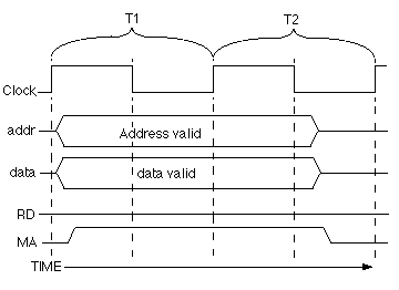
Fig. 16.6.4 shows a write operation on this same bus. The only changes are that the data is valid from the start because the bus initiator (often the CPU) is communicating this data value to the other device right off the bat, not requesting it and waiting for it to appear. Also, the RD wire stays low, indicating this is a write operation.