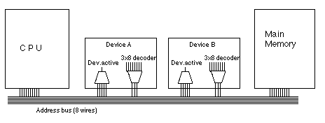
Fig. 18.7.1: Memory address space showing where two peripherals' registers are mapped
Another way of communicating with peripherals (through their controllers, of course) is to use the system bus and pretend that the registers in the device controller are words in memory. This clever idea, called memory-mapped I/O, because I/O devices are mapped into fixed regions of the memory address space, gives a potentially unlimited supply of virtual ports. Today it is the commonest way to do I/O and even computers that have explicit IN and OUT instructions with real ports augment their capacity with memory-mapped I/O. Some chips, like the Motorola 68000 which was used to power the early SUNs and Macintoshes, had no explicit I/O instructions, relying totally on memory-mapped I/O.
The term used by some authors to denote explicit I/O that uses IN and OUT instructions is isolated I/O, as opposed to memory-mapped I/O.
Fig. 18.7.1 shows the memory address space of a fictitious computer and where I/O peripherals have been assigned. There are 8 address bits, so there are only 256 addresses, from 00000000 up to 11111111. 8 of these addresses are allocated to device A while 8 others are allocated to device B. Memory gets all the rest. All the allocated words for a single device are contiguous, although main memory's addresses are not necessarily contiguous.
Fig. 18.7.1: Memory address space showing where two peripherals' registers are mapped
The words of memory that are set aside for an I/O controller are equated to its control registers, which play the same role as the ports in section 2.
When the CPU wants to inspect an I/O controller's register, it issues a memory read to the system bus specifying the address that corresponds to that peripheral's register. When it wishes to give a command or send actual data, it issues a write to the memory word corresponding to the peripheral's register.
The memory is never really involved at all during these memory-mapped I/O operations. It completely ignores any read or write commands that specify addresses not within its range. Thus, the name of this type of I/O arrangement, memory-mapped I/O, is misleading because what is really mapped is the memory address, but memory address-mapped I/O is a mouthful and computer programmers are in a hurry.
How does memory-mapped I/O actually work? Every device that attaches to the system bus has a decoder that takes in the address wires and interprets them. If that address is within the range specified for that device, then an "activated" wire goes high, similar to the MA (memory active) wire of memory. If the address is not for that device, then the activated wire is low and the device ignores the bus. Main memory also has a decoder that enables it to ignore the read and write commands that are meant for peripheral devices.
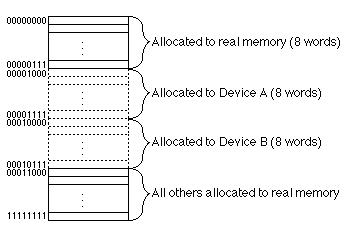
Fig. 18.7.2 shows a system with two peripherals, the CPU and main memory.
Fig. 18.7.3 shows the gates in the decoder of each device which set the activated wires. Each device also has a decoder that determines the specified address that is on the address bus, just as with main memory.
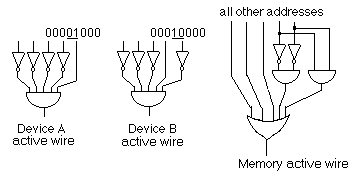
Fig. 18.7.3: Decoder logic for device active wires;
refer to Fig. 18.7.1 for the addresses
Once memory-mapped I/O is in place, the algorithm for communicating with a peripheral is essentially no different from the earlier example that used IN and OUT. Instead of IN, the CPU issues a LOD instruction to fetch a word from "memory" and instead of OUT, it issues a STD instruction. The addresses given are the mapped addresses of the control, status and data registers of the peripheral's controller.
Fig. 18.7.4 is a reprise of Fig. 18.2.2, with the substitution of LOD and STD for IN and OUT.
In order to translate from the isolated I/O version to memory-mapped I/O, we have to know where the "registers" are in memory. Following is an assignment of three memory words to the three registers needed for a tape reader:
      memory
      address  register   writer   reader    function
      ------   --------   ------   ------    --------
        128       0        CPU      TR       status of CPU
        129       1        TR       CPU      status of tape reader
        130       2        CPU      TR       command
        131       3        TR       CPU      data sent from tape reader
Here's the program:
          LDI  001b         ;form the code for the START command
          STD  130          ;send the START command to the tape reader
          LDI  01b          ;put the CPU's status into its status port
          STD  128          ;which the TR reads as "Go read for me now!"

WHILE1:   LOD  129          ;read data ready bit from status register
          SUB  DATAREADY    ;compare to "01"b
          JZ   ENDWHILE1    ;if equal, then done
          JMP  WHILE1       ;else go back to top of loop
ENDWHILE1:NOP               ;this is outside the loop, ready to go on

          LOD  131          ;read data byte in data register
          STD  X            ;store into main memory somewhere (X)
          LDI  10b          ;get ready to write 1 into data accepted
          STD  128          ;write to the CPU's status register
                            ;the tape reader is now spinning, waiting for CPU
          LDI  100          ;pause the loop to allow the tape reader
                            ;to catch up
WHILE2:   JZ   ENDWHILE2    ;waste 100 time units here
          SUB  ONE          ;by counting down from 100
          JMP  WHILE2       ;to 0 by subtracting 1
                            ;... sometime inside here the tape reader sets
                            ;    its status register back to "00"
ENDWHILE2:NOP

          JMP  WHILE1       ;do it all over again to read next byte

DATAREADY:NUM  01b          ; 01b is the code for the CPU saying "I'm waiting!"
ONE:      NUM  1
Fig. 18.7.4: Polling program to read bytes from device A, using memory-mapped I/O