Practice Exercise 4 Answers
-
Implement the following two Boolean functions using the blank PLA below.
Label the outputs and inputs clearly.
               Cout = A'BC + AB'C + ABC' + ABC
               Sum = A'B'C + A'BC' + AB'C' + ABC
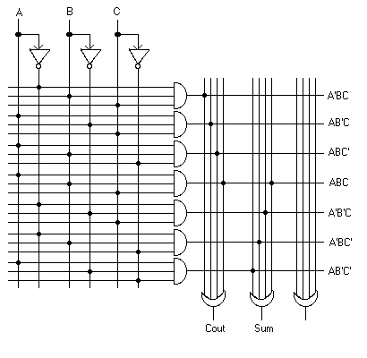 Since the term ABC is used twice, once for Cout and once for Sum, it can be
reused in the actual circuit, too. This is why the horizontal line for ABC
has two solder points on it, connecting it to the OR gates for both
Cout and Sum.
Since the term ABC is used twice, once for Cout and once for Sum, it can be
reused in the actual circuit, too. This is why the horizontal line for ABC
has two solder points on it, connecting it to the OR gates for both
Cout and Sum.
-
A Priority Encoder (PE) is like an encoder except that it allows more
than one of its inputs to be high simultaneously. All the inputs have a
numerical label, from 0 up to n-1, if there are n input wires. The PE
outputs the binary number, or address, of the input which has the highest
numerical label. In addition, it has an output status wire which is 0 or 1
to indicate whether or not any of the inputs has the value 1. This is
necessary because if none of the inputs is 1, then the value of the output
binary number would be bogus, even though it would be some binary number.
Following is the truth table for the priority encoder and the minimized
minterm expressions that implement the three output functions.
          I0     I1     I2     I3    |    B1     B0     S
          ---------------------------+--------------------
           0      0      0      0    |    0      0      0
           0      0      0      1    |    1      1      1
           0      0      1      0    |    1      0      1
           0      0      1      1    |    1      1      1
           0      1      0      0    |    0      1      1
           0      1      0      1    |    1      1      1
           0      1      1      0    |    1      0      1
           0      1      1      1    |    1      1      1
           1      0      0      0    |    0      0      1
           1      0      0      1    |    1      1      1
           1      0      1      0    |    1      0      1
           1      0      1      1    |    1      1      1
           1      1      0      0    |    0      1      1
           1      1      0      1    |    1      1      1
           1      1      1      0    |    1      0      1
           1      1      1      1    |    1      1      1

              S = I0 + I1 + I2 + I3

              B0 = I1I2'I3' + I3

              B1 = I2 + I3
-
Following is a 2-input, 2-output half adder circuit which can be used to
build a full adder circuit. C is the carry bit, and S the sum bit. Verify
by truth table that this circuit does indeed perform the half adder
function.
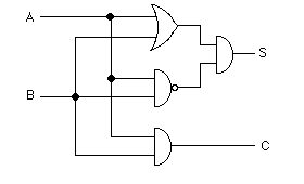 Here's the truth table worked out for the circuit, and it conforms exactly
to the standard half adder truth table. An abbreviated NAND truth table is
shown to the right for ready reference when calculating.
Here's the truth table worked out for the circuit, and it conforms exactly
to the standard half adder truth table. An abbreviated NAND truth table is
shown to the right for ready reference when calculating.
               A     B    |   S      C               NAND
               -----------+------------             ------
               0     0    |   0      0                1
               0     1    |   1      0                1
               1     0    |   1      0                1
               1     1    |   0      1                0  (A=B=1)
-
Following is a full adder circuit using the half-adder of problem 3
as a subcircuit:
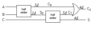 Assuming that this is used as a bit-slice in an n-bit adder, what would
the delay of such an adder be? Would it be better than the bit-slice used
for the calculations in chapter 4?
(Treat NAND and NOR as having a delay of 1d.)
The delay is 4d for the above circuit. The delay of the half adder box
is 2d for S and 1d for C, so we can arrive at our values given on the
various lines in the picture.
In an n-bit adder, the sum would be ready after 4nd. The version shown in
chapter 4 is 6d + 2(n-1)d or 2nd + 4d, which is less than 4nd if n>=3, so
this new version above is slower.
Assuming that this is used as a bit-slice in an n-bit adder, what would
the delay of such an adder be? Would it be better than the bit-slice used
for the calculations in chapter 4?
(Treat NAND and NOR as having a delay of 1d.)
The delay is 4d for the above circuit. The delay of the half adder box
is 2d for S and 1d for C, so we can arrive at our values given on the
various lines in the picture.
In an n-bit adder, the sum would be ready after 4nd. The version shown in
chapter 4 is 6d + 2(n-1)d or 2nd + 4d, which is less than 4nd if n>=3, so
this new version above is slower.
-
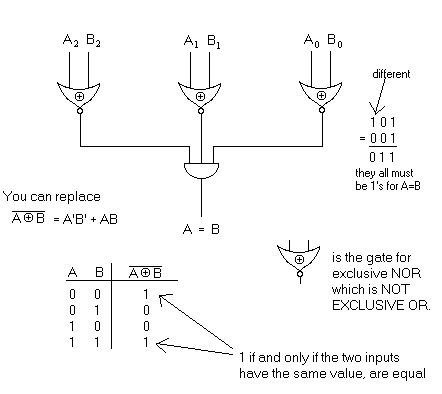
Draw a circuit diagram that implements a comparator function of two
3-bit binary numbers. The comparator puts out a 1 if and only if all of the
pairs of inputs are the same bit value. Label the inputs
A0,
A1,
A2 and B0,
B1, B2.
In order for the comparator to put out a 1, the following must be
true: A0=B0,
A1=B1
and A2=B2.