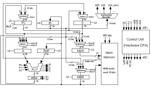
Below is a diagram of the CPU, which we will explain in detail. Such diagrams are called block diagrams because they show the major functional units without delving into the individual gates.
Each of the smaller rectangles are registers, composed of 16 flip-flops, except for the MAR, which is 12 flip-flops. They have 16 input wires and 16 output wires, one per flip-flop. In addition, there is a load wire which is connected to the CK wires of each flip-flop. The register stores a new value only when this load wire goes high. Fig. 7.1.2 shows a block diagram of a 16-bit register.
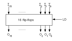
Fig. 7.1.2: Block Diagram of a 16-bit register with load wire
In addition to the load wire, some registers have a clear wire which when high puts 0 into every flip-flop of the register. One register, PC, contains an increment wire which when set high adds 1 to the binary number contained in the register. Though this sounds like there would need to be an extra adder just for this register, it is relatively easy to build a register which does this; a full adder is not required, merely some AND gates to propagate the carry through the register's flip-flops. In Fig. 7.1.3 we show the block diagram for one of these "super registers."
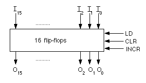
Fig. 7.1.3: Super Register with load, clear and increment wires
There are seven registers in CSC-1:
| A | accumulator | stores the result of arithmetic operations as well as one of the operands |
| TMP | temporary | stores the second operand of arithmetic operations |
| S | secondary | a temporary storage place for accumulator values, most often used in calculated memory addresses for indirect loads and stores |
| PC | program counter | contains the address of the next instruction in memory to be executed. |
| IR | instruction register | contains the actual instruction which is being currently executed. |
| MAR | memory address register | contains the address of the memory word to be read or written |
| MBR | memory buffer register | contains the value of the word to be written into memory, or the value of the word just read from memory |
The MAR and MBR are old friends, and work just as described in Chapter 6. Here are some statistics on the CSC-1:
| Size of MAR = 12 bits | This implies that there are 4096 words in memory. |
| Size of MBR = 16 bits | Each word of memory is 16 bits wide. Thus the CSC-1 is not byte addressable, but rather word addressable. |
| All other regs = 16 bits wide | One word of memory fits snugly into A, S, PC, IR, or TMP |
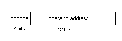
The instruction register is divided into two sections conceptually, but not physically. Fig. 7.1.4 shows this division. The first four bits are commonly called the opcode, short for operation code. The contents of these bits form a 4-bit binary number which tells the control unit which instruction to perform. The remaining 12 bits form the operand, which is either a 12-bit binary number or an address.
The opcode field being 4 bits long implies that there can only be 16 instructions, since 24 = 16. However, there are more than 16 instructions in the CSC-1, 24 to be exact. But 9 of these do not require an operand. Thus, their opcodes can be longer than 4 bits. Because the computer needs to know when to interpret the remaining 12-bits as operand or part of the opcode, one of the opcodes, 1111, is reserved to mean "what follows is not an operand, but part of an extended opcode" for those instructions which need no operand.