Section 7.6
Example of control points and the fetch/decode/execute cycle

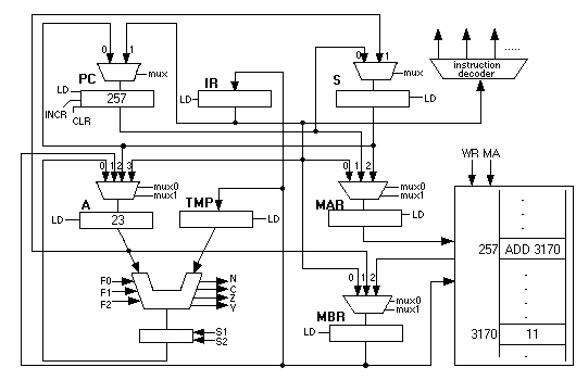
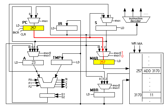
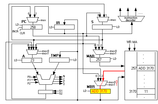
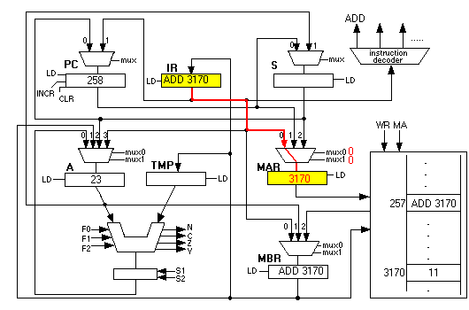
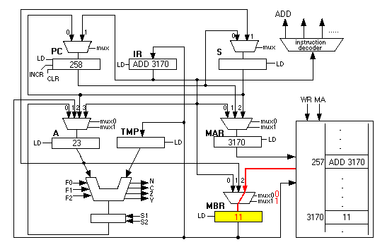
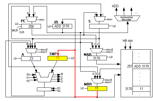
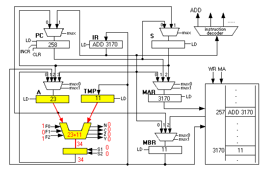
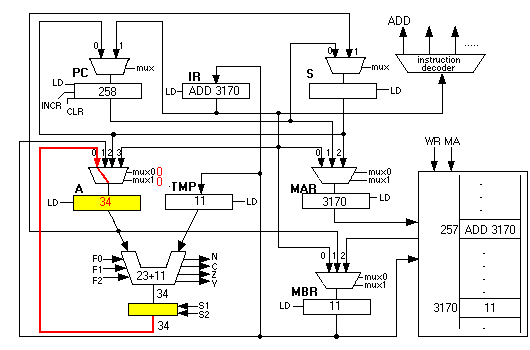
Let us go through one complete ADD instruction in tedious detail so we can see how the control points are set during the stages of the instruction cycle. Some of the extraneous lines have been omitted from the block diagrams to make the picture clearer.

  1. The beginning of the cycle, PC has the address 257. Memory word 257 contains a bit pattern that we can interpret as ADD 3170. The bit pattern is actually 0011110001100010. The first four bits 0011 are the ADD instruction, while 110001100010 is the binary number 3170.

  1. The first thing to happen is to set the MAR-MUX so The MAR-MUX is set so that PC's output is copied into MAR when MAR-LD goes high. This puts the address of the next instruction into MAR:

  1. At this point, the PC-INCR wire goes high, followed briefly by PC-LD, which causes the value of PC to be incremented by 1. This sets up the machine so that the next instruction to be done will be the next one in sequence, at the next word in memory. If the instruction is a jump of some type, the value in PC will be completely overwritten later, so it doesn't hurt to add 1 to the PC. This step is usually done in parallel with the next step in order to save time by telescoping non-interfering actions together.

  1. Next MA (memory active) is set to 1, WR=0 to indicate this is a read and not a write, and the memory is given enough time to go fetch the needed value.

  1. Eventually the memory deposits "ADD 3170" into the MBR.

  1. This is then copied to the IR. MA is set to 0. This is the end of the instruction fetch stage.

  1. The value in IR is broken down by the opcode decoder, which sees that 0011 (the first 4 bits) are the ADD instruction. It "knows" that the last 12 bits are then the operand address so it will set up the wires to fetch the value. The decoder causes the ADD wire to go high. This is the operation decode stage.

  1. The lower 12 bits of the IR are copied into MAR (the top 4 are ignored; the MAR is only 12 bits long anyway), which is the beginning of the operand fetch stage. The operand is located inside memory word 3170, and is the value 11.

  1. Then the MA wire is set to 1 again to initiate another memory read.

  1. We wait for memory, which eventually puts the value 11 into the MBR.

  1. Then we set TMP-LD high which copies the MBR into TMP, and turn off MA. This is the end of the operand fetch stage.

  1. The appropriate code for addition (101) is fed into the F wires which control the ALU's function, and the contents of A and TMP are added together. The CNVZ bits are all set when the new value is computed, too. This output immediately goes into the shifter, but its code (on the two S wires) is 00 so the new value 34 just passes its value through to the output.

  1. The output of the shifter is selected by the A-MUX wires; all other inputs to the A register are of course ignored. A-LD is turned on and the new value is latched into the A register. This is the end of the execute phase.

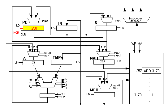
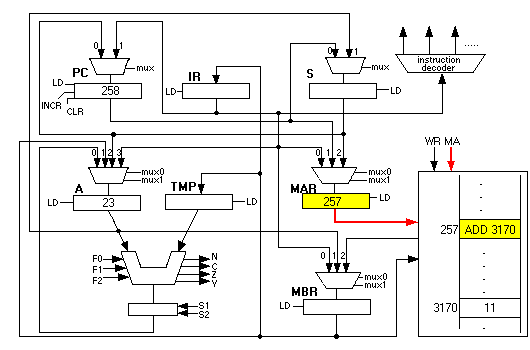
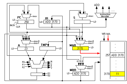
Now the computer is ready to begin the next instruction, which will be at location 258 (not shown in the pictures.)

Click here to see an animation of this entire cycle.

If the frames go by too fast, just wait because the animated GIF cycles back to the beginning again and again, until you click on the back button.

Different instructions cause different pathways to be chosen. For example, STD causes the value in A to be copied into MBR and then a memory write operation is activated. A doesn't get changed in the process, but some word of memory gets overwritten with A's value.

The control unit uses the current instruction to activate a sequence of pathways to get the proper job done. If the ADD wire is high, the sequence shown above is always done. If the STD wire is high instead, a different sequence is done. The first couple of steps, up through the instruction fetch stage and incrementing of the PC, are always done by every instruction, even HLT and NOP. From that point, differences occur depending upon which instruction is being performed.

A tiny but important point needs to be cleared up, especially since the above diagrams are a bit confusing. The output of a register is copied onto the wires that emanate from that register and the signals almost immediately travel to their destinations, which are usually muxes or other registers. However, these values are not latched into the registers until the LD wire goes high. Moreover, when there are several inputs to a mux, only one is selected by the associated mux select wires.

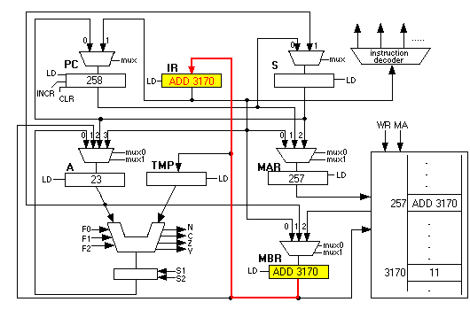
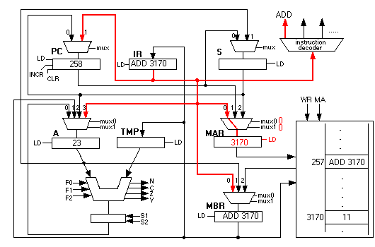
The above pictures only show in red those pathways that are of interest to us. Below is one of diagrams shown as it "really is." The output of the IR register is about to be copied into the MAR. Notice that every wire that emanates from IR is colored red and thickened a bit. These wires go into the PC's mux, A's mux, the MAR's mux, the MBR's mux and the instruction decoder. However, PC is not changed because PC-LD is not high. Neither are A or MBR changed because their LD wires are 0. Only MAR is changed. The instruction decoder is always "reading" the top 8 bits of IR and setting the appropriate instruction wire high, ADD in this case. But as long as IR's value doesn't change, it doesn't hurt anything for this decoding to happen continuously.

It is important to be aware of the way things "really are," even though we ignore some of the details in order to focus on the important aspects of the instructions' actions.