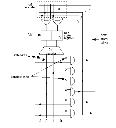
Fig. 7.8.1 shows a hardware DFA corresponding to the DFA given in Fig. 7.7.1.
The heart of the DFA is its state register, which has flip-flops to store the binary representation of the current state number. Since there are four states, 2 flip-flops are needed. A 4x2 encoder is shown exposed at the top, feeding into the state register, which gets a new value only when CK goes high. It is this CK wire which is tied directly to the computer clock.
Notice that wire 0 is not hooked to any of the inputs going into the OR gates because to write a 0 into the state register, none of the wires should have a 1 on it. In fact, the 0 wire is redundant and could be omitted.
A 2x4 decoder takes the output of the state register and sets one wire to 1. Thus, each state has its own unique wire.
The conditional selection of the next state happens by ANDing the current state wire and hooking this to one of the input wires. For example, in Fig. 7.7.1, the DFA specifies that if we are in state 2 and "c" is true, then the next state should be 3. Thus, we AND state 2's wire with the "c" wire and hook that into the 3 input wire. However, 3 will get stored into the state register only when CK goes high at the next cycle.
The state wires coming out of the DFA are used to set the control wires, such as MAR-LD, PC-INCR, F0, A-MUX1, etc. Many of these control wires must be activated at several different times or by several different situations. AND and OR gates are used to filter and combine these situations that lead to setting the control wires.
Fig. 7.8.2 shows two different control wires, S0 and MAR-LD, and how they are set. S0 is only set when the SHR (shift right logical) is executed, and then only during the execute phase of the instruction. Thus, these two wires must be ANDed together in order to set S0. Recall that SHR comes directly from the instruction decoder, as shown in Fig. 7.7.3. S0 is 0 at all other times, so the one AND gate is sufficient to give it a value.
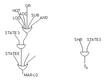
Fig. 7.8.2: How state and opcode wires feed into control points
However, MAR-LD is used much more frequently, and in a variety of settings. It is used during the initial instruction fetch part of the machine cycle, which is represented by STATE0. It is also set during the operand fetch step, STATE3, but only when the instruction is one of those that calls for an operand out of memory, namely LOD, ADD, SUB, AND, OR, NOT. Hence an OR gate tells if any of these instructions are being executed, and the output of this gate is ANDed with STATE3 coming out of the DFA so that this is only done at the proper moment in the fetch/decode/execute cycle. This wire is ORed with other conditions, such as STATE0, because the MAR must be loaded at other times. This leads to the complicated circuit shown in Fig. 7.8.2, which is not complete.
Hopefully by now you are sufficiently impressed with the complexity of a computer, at least the CPU, which is the heart of the computer. I/O devices and buses are another matter entirely, and are full of their own Byzantine layer upon layer of complexity. However, computer hardware designers have striven to reduce the complexity to manageable levels by employing regularity at every turn. Mathematics also helps a great deal. For instance, DFAs are a purely mathematical construct that can be applied to many real-world situations, including design of the control unit.
In chapter 9 we will look at small programs written in CSC-1's assembler language just to get a feel for how real programs are put together from these incredible minuscule and simple-minded instructions.