Practice Exercise 7 Answers
-
Encode the following instructions into CSC-1 machine language, using the
16 blanks provided for both the opcode and the operand.
They have been broken up into 4 groups of 4 merely for your
convenience and readability. If there are any errors, point them out and
tell why.
             JMP  2300     1 0 0 0   1 0 0 0   1 1 1 1   1 1 0 0

             ADD  5        0 0 1 1   0 0 0 0   0 0 0 0   0 1 0 1

             LDI  15       0 0 1 0   0 0 0 0   0 0 0 0   1 1 1 1

             STD  6270        6270 is too big for 12 bits

             RET           1 1 1 1   0 0 0 1   0 0 0 0   0 0 0 0

             JC  256       1 0 1 0   0 0 0 1   0 0 0 0   0 0 0 0

             HLT           1 1 1 1   1 0 0 1   0 0 0 0   0 0 0 0

             JNZ  2300        no such instruction as JNZ

             AND  4095     0 1 0 1   1 1 1 1   1 1 1 1   1 1 1 1
-
Suppose that a hardware designer sees the falling prices of memory and
decides to double the size of the CSC-1's memory to 8192 words. Each word
of this memory still has 16 bits each. What kinds of problems will arise?
Addresses will now be 13 bits wide, instead of 12 bits. This will require
expanding the MAR's size to 13. The real problem occurs when we realize we
can't squeeze 13-bit addresses into the existing command structure. We have
too many instructions, each with its own distinct opcode, to fit into 3
bits. And our memory words are still 16 bits wide, not 17. The most likely
fix is to let some machine instructions take up 2 words of memory, not just
one, which would change the fetch/decode/execute cycle, making it more
complicated.
-
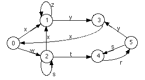
Following is a DFA. Sketch out a hardware DFA that implements this,
using the same basic structure as the hardware DFA in Fig. 8 of Chapter 7.
-
How to fix the hardware DFA.
a.) What happens if none of the condition wires (a, b, c...) have a 1 on
them?
None of the 4 inputs to the OR gates will be 1, so the ORs will all output 0
and 00 goes into the state register.
b.) How could this problem be fixed?
Do not allow CK to load a new value into the flip-flops until at least 1 of
the condition wires is 1. Use an OR gate (OR all these condition wires
together) and AND that with CK, using the output of the AND gate to control
loading the state register flip-flops. See diagram below.
-
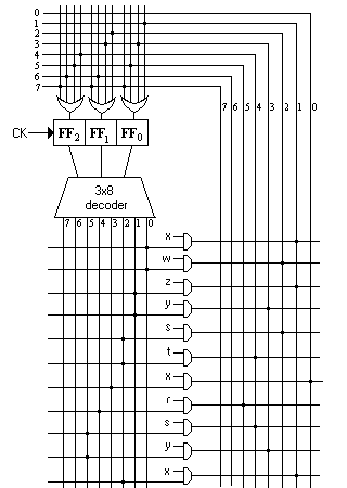
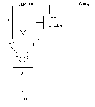
The "Super Register" discussed in Chapter 7shows three
"commands," namely LD (load), CLR (clear, or set all bits to 0) and INCR
(increment, or add 1). Show just one bit of the super register, with a
flip-flop at the center,
I3 coming in,
O3 going out,
and the carry from the
previous bit. The tricky part will be to show the ANDs and ORs that allow
only that command to be carried out.
-
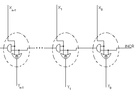
Incrementer circuits are very handy to have. The following circuit
takes in n wires, which form a binary number, and if the INCR wire is high,
outputs the binary number plus 1. If INCR is 0, the original number is
passed through unchanged. The crucial gates that implement this
incrementing function are contained in the dotted circles, which you must
fill in. They are all the same, so just show what one of them looks like.