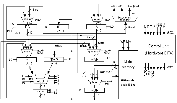
Fig. 8.1.1 is again the block diagram of the CSC-1 computer:
In the discussion that follows we will go through all of the wires. Some of this material is redundant from chapter 7, but it is repeated here for completeness and ease of reference.
All wires in the diagram are assumed to be single wires unless there is a slash through the wire with a number next to it, which indicates how many wires there are in the group. Thus, the line coming out of the PC register is slashed with 16, meaning there are 16 different wires coming from the PC register.
Each wire is labeled, although the full names are often implied. The several wires labeled "LD" are really different wires; their full names are prepended by the register into which these wires go. For example, the LD wire going into PC is really called "PC-LD", and the two multiplexor control wires going into the MBR's mux are MBR-MUX1 and MBR-MUX0.
For mux control wires, 1 is the most significant bit and 0 is the least. Each data input to a mux is labeled from 0 up to 3, or 2 or 1 if there are fewer inputs. For those muxes with more than two data inputs (A-MUX, MAR-MUX and MBR-MUX), the input is selected according to the binary number that MUX1/MUX0 form. To illustrate, suppose that we desired the MAR to get the output of S. The wire from S-OUT to MAR-MUX is labeled 2, which is 10 in binary. Thus, MAR-MUX1 must be 1 and MAR-MUX0 must be 0. We will call the several inputs to a MUX its ports. Thus, MARMUX has ports 0, 1 and 2.
The wires coming from registers are labeled by their register's name followed by OUT. Thus, A-OUT, S-OUT, MBR-OUT. The memory has a set of 16 wires which it uses to send data to the MBR register. These are labeled MEM-OUT. All these OUT wires can be referred to individually by number: A-OUT0, S-OUT14, and MEM-OUT3. All registers except MAR are 16 bits wide, so their outputs are labeled 0 to 15. The MAR has 12 bits.
The main memory has two sets of input wires: one set of 12 from the MAR register (MAR-OUT0 to MAR-OUT11) and another set of 16 from the MBR (MBR-OUT0 to MBR-OUT15). There is also a set of 16 output wires going into the MBR-MUX.
The PC register is different from the others in that it has two additional input control wires. One is labeled PC-INCR. When both PC-INCR and PC-LD are 1, the binary number in the PC register goes up by one. Overflow is ignored and the numbers wrap around. Put another way, if PC contains 1111111111111111 (16 1's), and PC-INCR=1 and PC-LD=1, the new value will be 0000000000000000 (16 0's). There is also a PC-CLR input which puts 0 in the PC register, when PC-LD is high.
Memory has two control wires, MA (memory active) and WR (write). If MA=0, the memory is isolated from all of its inputs and outputs. If MA=1 and WR=0, the selected word of memory is copied into onto MEM-OUT, which can then be latched into the MBR register when MBR-LD goes high. If MA=1 and WR=1, the value in the MBR is copied into the selected word of memory. Of course, the value in the MAR register determines which word is read or written.
In some cases only some of the wires in a wire group are used as input and these are labeled as N lsb or N msb at the point where the wire group goes into the register. "lsb" stands for "least significant bits" meaning the lesser N bits of the wire group, as defined by the order of the flip-flops of the register from which they originate, and "msb" stands for "most significant bits," analogously.
Here are the exact wires that route into several components:
IR-OUT0 to IR-OUT11     go into port 0 of MARMUX
IR-OUT0 to IR-OUT11     go into port 1 of MBRMUX
PC-OUT0 to PC-OUT11     go into port 1 of MARMUX
S-OUT0 to S-OUT11       go into port 2 of MARMUX
IR-OUT8 to IR-OUT15     go into the instruction decoder
The ALU is controlled by the three wires F0, F1 and F2. These form a binary number between 0 and 7. Here is what they tell the ALU to put on its output wires:
F2 F1 F0
-------------------------------------------------------------
0  0  0     identity A     pass through A's value unchanged
0  0  1     identity TMP   pass through TMP's value unchanged
0  1  0     A and TMP      bitwise Boolean AND of A and TMP
0  1  1     A or TMP       bitwise Boolean OR of A and TMP
1  0  0     not TMP        bitwise Boolean NOT of TMP (A ignored)
1  0  1     A + TMP        arithmetic addition of A and TMP
1  1  0     A - TMP        arithmetic subtraction of A and TMP
1  1  1     unused
The shifter is controlled by the two wires S1 and S2. These form a binary number between 0 and 3. Here is what they tell the shifter to put on its output wires.
S1 S2
------------------------------------------------------
0  0     do nothing           pass input to output unchanged
0  1     right shift 1 bit    logical shift only
1  0     left shift 1 bit     logical shift only
1  1     unused
There are 16 data outputs of the ALU, collectively called ALU-OUT. The condition outputs C, N, Z and V of the ALU signify the following conditions.
C     Final carry-out of the adder is 1;
      signifies overflow if the contents of
      the registers are considered to be unsigned.
V     Overflow of 2's complement numbers
Z     All output wires have 0
N     The value is negative when viewed as a 2's
      complement number (ALU-OUT15=1)