Practice Exercise 8 Answers
-
Write out the control points for the SUB instruction. Use the
microprograms in Chapter 8 as a model.
The answer to this is almost too easy. The control points for SUB would
look almost exactly like ADD, except the ALU function would change from
F=101 to F=110, as shown below.
               1.     MAR-LD=1
               2.     MAR-LD=0;  MA=1;  WR=0;  MBR-MUX=10
               3.     MBR-LD=1
               4.     MBR-LD=0;  MA=0;  PC-INCR=1;  IR-LD=1
               5.     IR-LD=0;  PC-LD=1
               6.     PC-INCR=0;  PC-LD=0;  MAR-MUX=00
               7.     MAR-LD=1
               8.     MAR-LD=0;  MA=1;  WR=0;  MBR-MUX=10
               9.     MBR-LD=1
              10.     MBR-LD=0;  MA=0;  TMP-LD=1
              11.     TMP-LD=0;  F=110;  SH=00;  A-MUX=00
              12.     A-LD=1
              13.     A-LD=0;  MAR-MUX=01
-
Write out the control points for the STD instruction.
The STD instruction does not have an operand fetch phase. Instead, the
value in the A register is copied to memory using the address X in the lower
12 bits of the IR. Once the instruction has been loaded into the IR in step
5 and once PC has been incremented, A's output is directed to the MBR as
input (MBR-MUX=1). Then MBR is loaded from A. However, we also need to
copy the low 12 bits of the IR (which is where the instruction is) into the
MAR before we activate memory. We can load the MAR and the MBR in parallel,
because their new values are coming from different registers.
Once both the MAR and MBR have the right
values, we activate memory
with a WRite command. In step 9, MAR-MUX is set to 01 to get it ready for
the next instruction.
               1.     MAR-LD=1
               2.     MAR-LD=0;  MA=1;  WR=0;  MBR-MUX=10
               3.     MBR-LD=1
               4.     MBR-LD=0;  MA=0;  PC-INCR=1;  IR-LD=1
               5.     IR-LD=0;  PC-LD=1
               6.     PC-INCR=0;  PC-LD=0;  MBR-MUX=01;  MAR-MUX=00
               7.     MBR-LD=1; MAR-LD=1
               8.     MBR-LD=0;  MAR-LD=0;  MA=1;  WR=1
               9.     MA=0;  WR=0;  MAR-MUX=01
-
Explain what would have to be done to implement the RTL for any of the
jump instructions of the CSC-1, for example, JZ:
If Z=1 then PC <- x
In order to implement a JZ, you need to set PC-MUX to 1 so that the
lower 12 bits of the IR are copied into the PC, and you also need to set
PC-LD to 1 only on the condition that the Z wire is 1. This can be done by
using an AND gate, as drawn below, and also in RTL in the following way:
PC-LD=Z & JZ
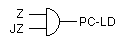 meaning that instead of piping a plain 0 or 1 into PC-LD, we take the
values on the two wires Z and JZ and AND them, sending the output of this
into PC-LD. Remember that the JZ wire is one of the outputs of the
instruction decoder and will have a 1 on it when the current instruction is
JZ.
Of course, PC-LD is set high by other combinations, too, and these are
formed by ANDing the output of the above AND gate with other instruction
wires, as hinted at the very end of Chapter 7.
meaning that instead of piping a plain 0 or 1 into PC-LD, we take the
values on the two wires Z and JZ and AND them, sending the output of this
into PC-LD. Remember that the JZ wire is one of the outputs of the
instruction decoder and will have a 1 on it when the current instruction is
JZ.
Of course, PC-LD is set high by other combinations, too, and these are
formed by ANDing the output of the above AND gate with other instruction
wires, as hinted at the very end of Chapter 7.
-
There is no JNZ instruction. How could you simulate the effect of it?
JNZ can be simulated by using a JZ instruction to jump around a
non-conditional jump, namely JMP, in the following way:
                  JNZ  X                        JZ     Y
                  ....                          JMP     X
                  ....                   Y:     ...
                  ....                          ...
          X:     other code              X:     other code
The code on the left is what you'd like to be able to write directly but
cannot because there is no JNZ instruction. However, the code on the right
does the same thing. It just is longer by one instruction and uses a new
label, Y.
-
There is no CLR (clear) instruction in the CSC-1 instruction set.
Explain how this could be implemented.
A CLR instruction would put 0 into the A register. This could be done
in two ways:
                  by loading 0 from a word in memory
                  by subtracting the current contents of A from itself.
The trouble with the memory solution is that it ties up a word of memory
and you must make sure that the value 0 is never changed in that word, which
would be tough.
The second solution is easy but a bit tricky because you have to copy A's
value into the TMP register somehow. This can be done by copying A into the
MBR, and then loading TMP from the MBR. Then use the subtraction code in
the ALU, F=110.
-
Operating system programmers often need a SWAP instruction which, in one
single uninterruptible instruction, can exchange the value in A with the
indicated word of memory. In effect, it does both a load and a store in one
single instruction. The assembler format is
SWP x
where x is an address of memory. Write the RTL statements that would do this.
The RTL for SWP would be:
A <- m[x]; m[x] <- A
Notice that this implies that the MBR is copied into the A register while
the A register is simultaneously
copied into the MBR. You cannot do one of
these before the other -- they must somehow be done simultaneously.
-
The RTL of question 6 seems to imply an impossible task. List two ways
it can be accomplished.
Obviously, the simultaneity of the RTL for SWP looks impossible, yet
because of the way that flip-flops work, it is actually quite simple. Since
there are direct data pathways A?MBR and MBR?A, all you need to do is to
choose these two pathways and then at the same time strobe the LD wires for
both A and MBR. This is one of the reasons why edge-triggered devices such
as flip-flops are preferrable over level-triggered devices such as pure
latches.
Another solution would be to use a third register, such as the TMP
register, as follows:
               TMP <- m[x]
               MBR <- A
               m[x] <- MBR
Of course, the first line implies that after a memory fetch, MBR is copied
into TMP. The same value, x, can stay in the MAR the whole operation.
-
Compare the organization of the CSC-2 shown in Chapter 8 to
the CSC-1 computer. Write down 1 pro and 1 con of this organization with
regards to the CSC-1 organization. That is, list one way it is better and
one way it is worse.
PROS: The CSC-2 organization is better than the CSC-1:
-
Every register is connected to every other register so you don't have to
make up special data pathways. Any connection is possible.
-
It's easy to increment (add 1 to) any register; just run it through the
adder with the +1 register as the other operand.
-
This organization is very flexible whereas the CSC-1 org. is rigid. You
can use almost any register as temporary locations.
CONS: The CSC-2 organization is worse than the CSC-1:
-
It is slow!!! If everything has to go through the main data path,
including the shifter and the adder, then it will take more time.
-
It is bigger and more expensive to build on a chip because there are more
gates and more wires.
-
Write out both the RTL and the control points for the STS instruction
for the CSC-2 computer, using the ADD instruction as a model.
The RTL and control points for the STS instruction for the CSC-2:
               MAR <- PC          A=2  F=0  SH=0
                                  RESULT-LD=1
                                  C=6

               PC <- PC + 1       A=2  B=1  F=5  SH=0
                                  RESULT-LD=1
                                  C=2

               MAR <- S           A=5  F=0  SH=0
                                  RESULT-LD=1
                                  C=6

               MBR <- A           A=4  F=0  SH=0
                                  RESULT-LD=1
                                  C=7

               write to memory    MA=1  WR=1  RESULT-LD=0