|
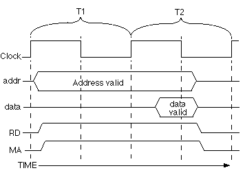
Fig. 16.6.2 shows a timing diagram for the bus when a read operation is occurring: This is really a graph showing activity on the various wires of the bus over time. Some wires are single lines, such as RD, MA and Clock. There are two voltage levels: high and low, with high being used to represent logic 1 and low being used to represent logic 0. The clock cycles back and forth between logic 1 and logic 0. |